Сурет:Wafertraksystem.jpg
Түпнұсқа файл (2048 × 1536 пиксел, файл өлшемі: 577 КБ, MIME түрі: image/jpeg)
| Бұл файл Wikimedia Commons? жобасынан, сондықтан басқа жобаларда да қолдануы мүмкін. Commons ашық лицензиялы медиа файл қоры. Сіз жобаға көмектесе аласыз. |
Ортаққордан қарау |
Түйін
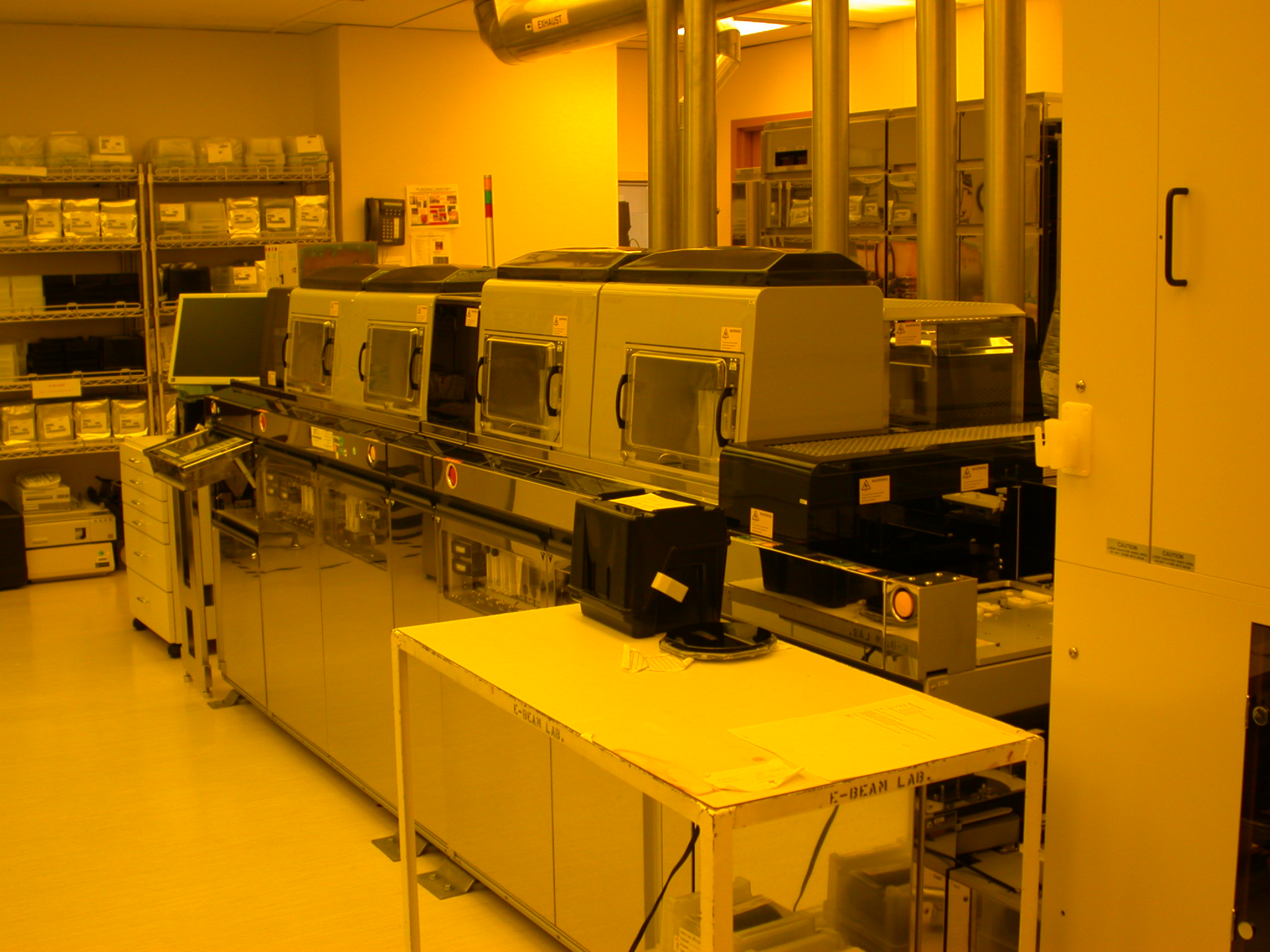
An aligner is a major piece of equipment used in semiconductor device fabrication. Trending from upper left to lower right is the wafer-track system of a photolithographic cell that uses the "i-line" from a mercury arc lamp (wavelength 365 nm) to expose photoresist deposited on silicon wafers. Wafers are robotically loaded from a carrier at the left hand of the system and progressively are coated with photoresist, exposed to ultraviolet light, and "developed". The development step involves using a solvent to remove either the exposed (positive photoresist) or unexposed (negative photoresist) portions of the film. In the foreground is a black plastic box containing silicon wafers with a diameter of 6" (150 mm).
Photo taken at HP Labs by Alison Chaiken using a Nikon 995 camera. Note that the light in the room really is yellow!
Лицензиялау

|
Бұл файлды GNU Free Documentation License лицензиясының 1.2 нұсқасы бойынша немесе ескі Ашық бағдарламалық жасақтаушы қорымен жарияланған нұсқасының шарттарына сәйкес көшірмесін алуға, таратуға және/немесе өзгертуге болады. Лицензия көшірмесі GNU Free Documentation License деп аталынған бөлімде көрсетілген. |
| Бұл файл Creative Commons Attribution-Share Alike 3.0 Unported лицензиясы бойынша қолжетімді. | ||
| ||
| Лицензияландырудың бұл қасиеті осы файлға GFDL лицензиясының жаңартылуының бір бөлігі ретінде енгізілген. |
Файл тарихы
Файл сол кезде қалай көрінгенін көру үшін күн/уақыт дегенге басыңыз.
| Күн/Уақыт | Нобай | Өлшемдер | Қатысушы | Пікір | |
|---|---|---|---|---|---|
| қазіргі | 07:11, 2006 ж. ақпанның 3 | | 2048 × 1536 (577 КБ) | Chaiken | An '''aligner''' is a major piece of equipment used in semiconductor device fabrication.Trending from upper left to lower right is the wafer-track system of a photolithographic aligner that us |
Файл қолданылуы
Бұл файлды мына бет қолданады:
Глобалды файл қолданылуы
Бұл файл келесі басқа уикилерде қолданылады:
- ar.wikipedia.org жобасында қолданылуы
- ca.wikipedia.org жобасында қолданылуы
- en.wikipedia.org жобасында қолданылуы
- es.wikipedia.org жобасында қолданылуы
- fa.wikipedia.org жобасында қолданылуы
- fi.wikipedia.org жобасында қолданылуы
- id.wikipedia.org жобасында қолданылуы
- mk.wikipedia.org жобасында қолданылуы
- pt.wikipedia.org жобасында қолданылуы
- tr.wikipedia.org жобасында қолданылуы
- uk.wikipedia.org жобасында қолданылуы